 A...HiRes..
 B...HiRes..
 C...HiRes..
 D...HiRes
Over the past 35 years I have been using a construction technique that I have not seen discussed much. These techniques are for the builders that like to experiment with circuit changes as they go along without having to start over with a new printed circuit board. I call it a "Hand Written Board" because it is not nearly as nice or reproducible as a "Printed Circuit Board". The "Dead Bug" and "Manhattan" style techniques fall into this same category in that they are fast and easily modified. Whereas those techniques are useful and very fast for bread boarding RF circuits, they get somewhat cumbersome when digital circuitry is involved because of the high density wiring. Also, these techniques do not yield very robust boards until the board is placed in a box. The technique that I will describe overcomes those difficulties.
The technique is based on a single side copper clad FR4 board from Vector. Figures A and B show the copper side and the unclad bottom respectively. The Vector and DigiKey part numbers are on the sticker. As you can see, this board is 4.5 X 17 X 0.062 inches and has 0.042 inch ID holes space on a 0.1 inch grid. They can be purchased readily from Mouser and Digikey. Vector, also, manufactures a smaller size but be SURE to get the FR4 material. The epoxy board is less expensive but cracks easily.
Figure C shows three colors of #30 solid wire wrap wire. This can be purchased at Radio Shack. The Blue is #278-503, the white is #278-502, and the red is #278-501. Each spool has 50 feet of wire.
Figure D are the basic tools that I use.
The hand drill is a Fiskars # 85116984 and can be obtained from Amazon.com
and other places. The drill bit shown is a # 40 numbered bit which
is 0.098 inches OD. Anything around that size is OK. The diagonal
cutters and needle nose pliers are very common and most already have them.
The wire stripper needs to be of good quality and capable of stripping
#30 solid wire. Many manufactures make such a tool. The one
shown in Figure D is a T-Stripper. Not shown is a soldering
iron with a small tip which most builders already have. I have found
that a temperature controlled tip is an asset.
A...HiRes..B...HiRes..C...HiRes..D...HiRes
This construction technique consists of mounting the components on the copper side of the board and doing point-to-point wiring on the other side. I use the hand drill and #40 bit to relieve the copper around the hole with a few gentle twists of the bit. They actually make tools for doing this, but I have found that they are sometimes too large for closely spaced components and the drill bit works better.
If you are mounting a component with a lot of leads, use a felt tip pen to mark the clearance holes and then relieve them all at the same time. If a component has a ground connection, then don't relieve the hole and solder the pin to the copper plane from the top. If the ground pin is not accessible, then connect it on the bottom with a small wire, run the wire through an adjoining hole and solder it on the top. If your circuit consists of a lot of discrete components and is not too dense, then just bend the leads and lap solder them together on the bottom of the board as shown in Figure H. If your circuit is digital with lots of leads or very complex, then use the wire wrap wire to make the connections on the bottom. I strip the wire and hold it next to the pin that I am attaching it to with the needle nose pliers. I then use the small screw driver to bend it around the pin. Having done that, I will hold it in place with the screw driver and then use the needle nose pliers to crimp it around the pin. I then solder it in place. If the pin already has something soldered to it, I find it best to bend the stripped part into a U, tin it with solder, and then heat the pin and wire as I slip it over the already soldered pin. With a little practice, one can make a lot of connections very fast. One example of a "Hand Written" board is shown in Figure E and Figure F
With some digital circuits, you need a low inductance power connection as well as a low inductance ground. The copper clad board creates the low inductance ground, but the #30 wire is not a very low inductance power plane. I have used copper tape on the non conductive side of the board to get around this problem as shown in Figure F. Be sure to solder any copper tape joints. The adhesive makes a good insulator!
If you have a circuit where high currents are flowing, #30 wire won't suffice. In those cases I have laid down copper tape on the bare side of a single sided copper board. The copper side is down so I fold copper tape around the edges and solder it to the copper side of the board. This forms a low inductance border on the bare side of the board. The higher current traces are then laid down with tape. You cannot solder too many time to the tape or the heat will render the adhesive ineffective. An example of this type of construction is shown in Figure G.
Figure H and Figure I show a small MMIC amplifier.
Figure J, K, L, M, N, O, P, and Q are some
examples of a more complicated set of boards (a 20m/40m transceiver that
I am building). You can tell from the empty relieved holes and the
solder spots all over the board that many changes have been made along
the building journey. This is one of the advantages of this technique.
Also, if long runs from one end of the board to the other are needed, a
twisted pair or small coax can be used.
 E...HiRes..
 F...HiRes..
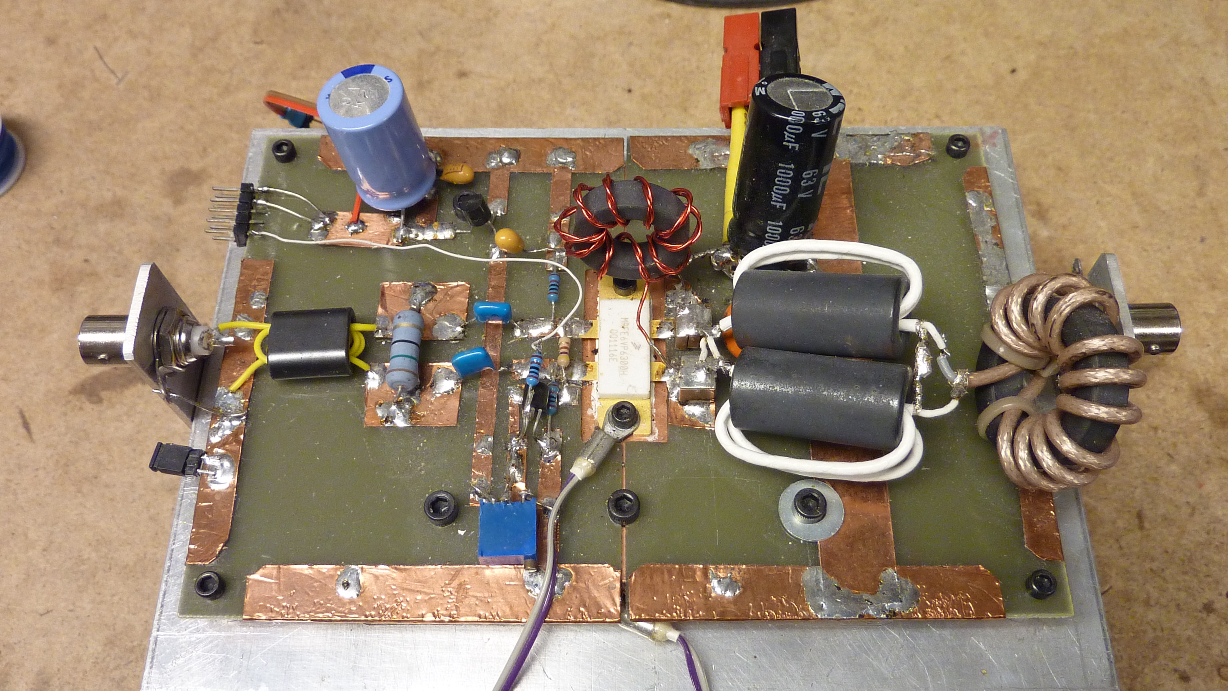 G...HiRes..
 H...HiRes..
 I...HiRes..
 J...HiRes..
 J...HiRes..
 L...HiRes..
 M...HiRes..
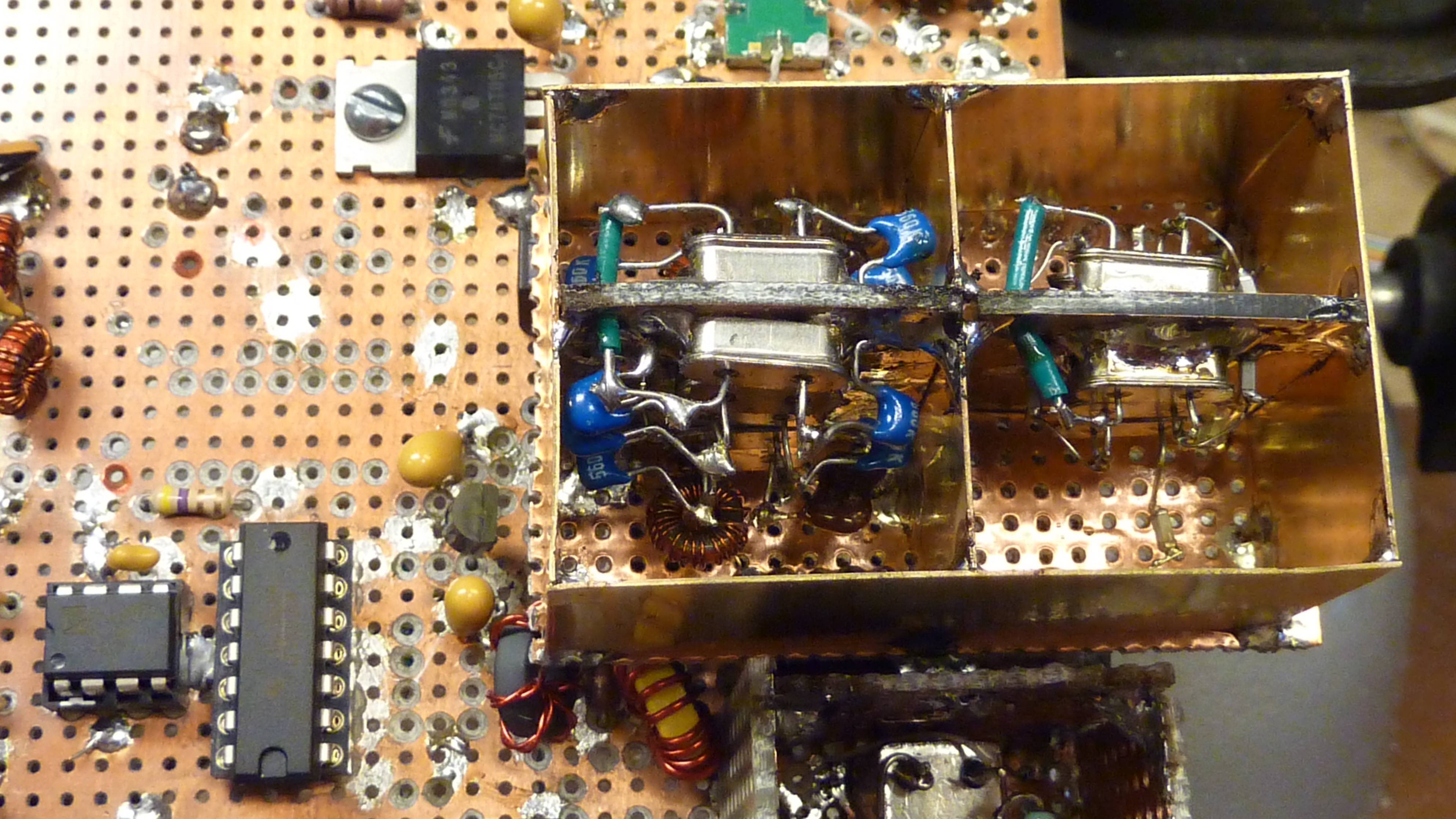 N...HiRes..
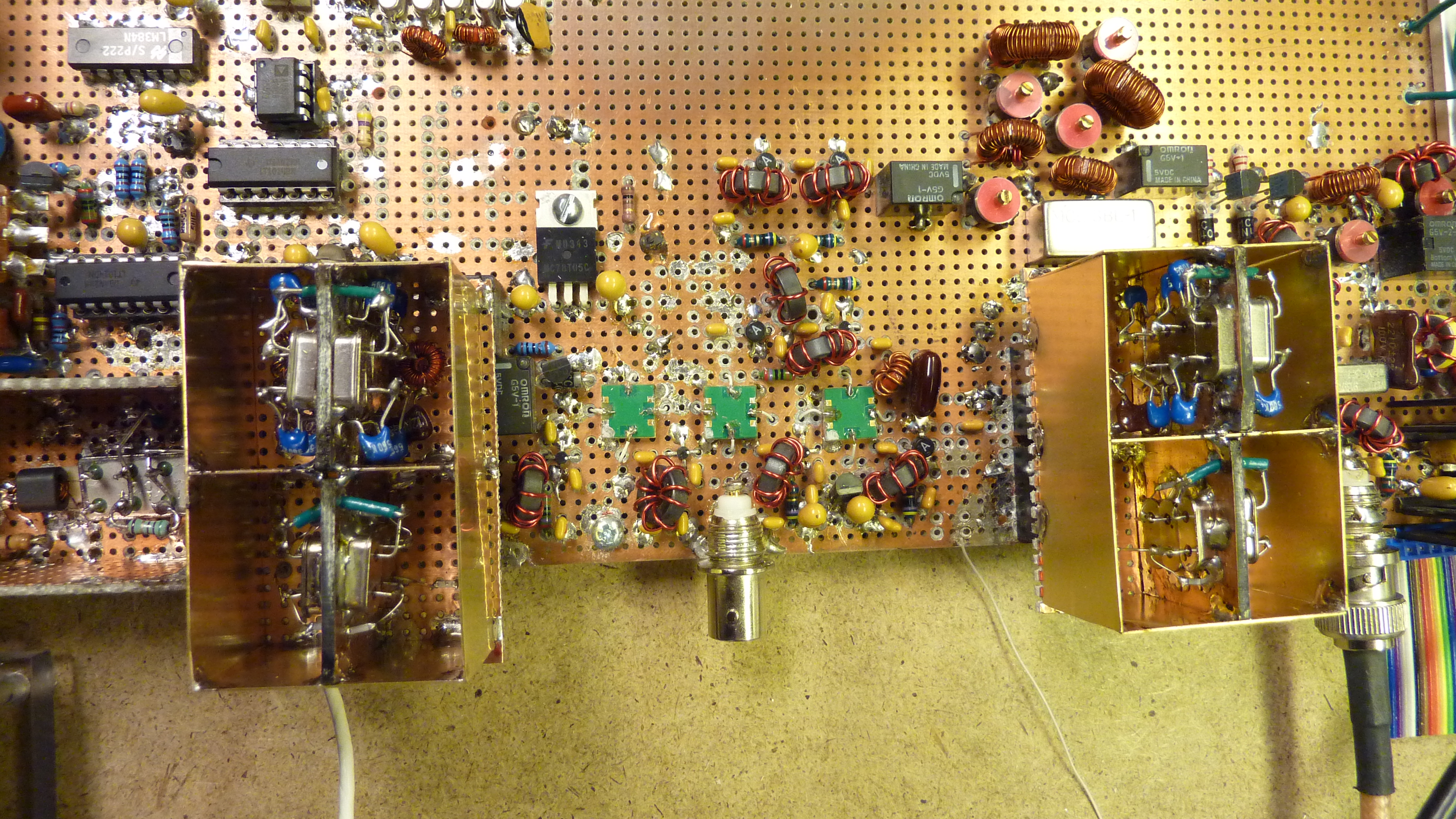 O...HiRes..
In summary, I have found this technique to be quite robust
and the layout density rivals that of a multi-layer PC board. From
an RF standpoint, the copper clad board offers good performance.
It's not pretty, but it works!
 P...
P... Q...
Q...